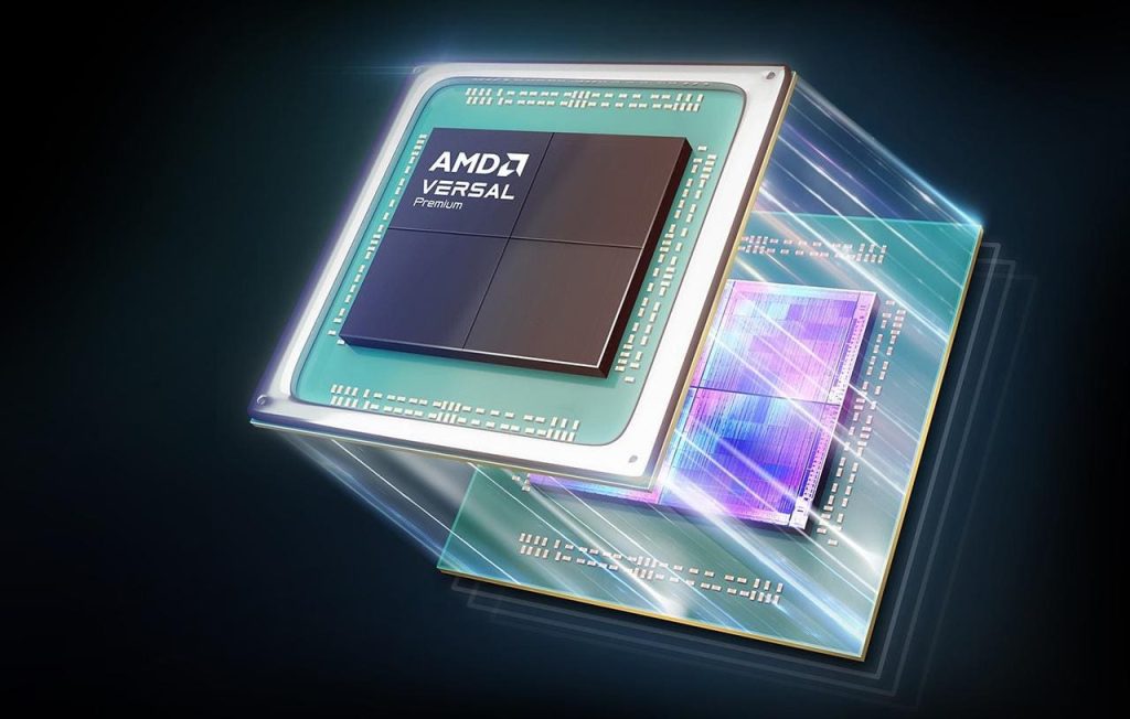
This morning, AMD marked yet another milestone with the announcement of its new Versal Premium VP1902 adaptive SoC (System On Chip) products. Semiconductor chip design is challenging and expensive. As such, there’s a lot of emulation, prototyping and verification work that goes into designing the next greatest processor, accelerator or platform product, and that’s where FPGAs (Field Programmable Gate Arrays) come in. You can think of FPGAs as both a virtual and physical sandbox for chip engineers to work in and emulate their designs in pre-production silicon, before committing to sending them out to expensive tape-out and chip fab processes for production ASIC (Application Specific IC) designs. The beauty of FPGAs is that they can mimic full, complex chip designs, but can also be reprogrammed as further optimization is achieved, new capabilities are added or chip errata is discovered and fixed.
Why Build The Worlds Largest Programmable, Adaptable Chip
A potential critical limitation with FPGA technology is packing the largest number of programmable logic gates on board, so engineers can design and emulate ever-larger, more complex chip designs for market applications like AI, which is driving insatiable demand for compute power and new functionality.
Built on TSCM’s 7nm process, AMD claims its new Versal Premium VP1902 adaptive SoC is the world’s largest, offering 18.5 million logic cells for 2X the programmable logic density and also delivering 2X the aggregate IO bandwidth compared to the previous gen Virtex UltraScale+ products. Relatively speaking, AMD’s nearest competitor, Intel, offers its Stratix 10 GX that tops out at 10M logic elements.
AMD achieved its Versal Premium logic density advantage with a new quadrant based architecture that relies on partitioning similar to that of a chiplet, though with VP1902, a high speed NoC (Network on Chip) connects multiple partitions that comprise the total functionality of the AMD-Xilinx Versal VP1902 FPGA. “Delivering foundational compute technology to enable our customers is a top priority. In emulation and prototyping, that means delivering the highest capacity and performance possible,” notes Kirk Saban, Corporate VP, Product, Software, & Solutions Marketing, Adaptive and Embedded Computing Group, AMD. “Chip designers can confidently emulate and prototype next-generation products using our VP1902 adaptive SoC, accelerating tomorrow’s innovations in AI, autonomous vehicles, Industry 5.0 and other emerging technologies.”
Debugging Performance And Software Tools Are Key For Customer Time To Market
In addition to the increased density and throughput of Versal VP1902, AMD notes its debug capabilities are “unmatched,” with the aforementioned NoC contributing to up to 8X faster debugging speeds than the previous gen VU19P FPGA portfolio. AMD has also bolstered its Vivado ML design suite of tools with new features that support development on VP1902 FPGAs, with automated design closure assistance, interactive design tuning, remote multi-user real-time debugging, and enhance back-end compilation of designs, all of which empower engineers with the ability to refine and improve their chip designs faster and with greater efficiency.
All in, AMD’s acquisition of Xilinx has continued to show clear synergy, with the adaptable nature of Xilinx technology permeating large swaths of the company’s combined product portfolio, from the client and cloud data center, to automotive, aerospace and AI markets and more. Though Versal is a core Xilinx technology that’s squarely targeted at applications where virtually no other solution other than an FPGA could address these unique, large-scale design challenges, it’s clear the combined team and technology portfolio continues to show strength and evolve.
AMD’s Versal Premium VP 1902 FPGAs will be sampling in Q3 ‘23 with production in the first half of 2024, along with software design tools available in the second half of 2023.
Read the full article here


